ELECTRONICS - [I2C Bus Scanner]

This page is about an 'I2S bus scanner' circuit. This circuit can be used to scan a certain I2C bus to find out all chips that are present on that I2C bus.
I2C is a bus system, invented by Philips, to communicate between chips on a PCB. The goal was to save wires (space) on the PCB. All devices on the I2C bus are interconnected with only 2 wires (SCL and SDA). Each device has its own hardware address. The master, usual a microcontroller, can establish a bidirectional communication with the other chips.
I2C uses a 7-bit addressing system so there are 127 possible addresses. My I2C scanner will try to address each one these 127 combinations. Only the chips that are present will respond with an ACK (acknowledge) pulse. My scanner uses this ACK pulses to determine if a chip is present. No other data or commands are transmitted.
My scanner can collect up to 30 different addresses. After the scan these addresses will be shown on a pair of 7-segment display modules. The addresses will appear in a hexadecimal format. The display will show the 7-bit addresses but a hardware jumper allows you to show the result as an 8-bit value.
I think an I2C scanner is very handy if you work a lot with I2C components like LCD modules or EPROM memory chips. You can use the scanner to test if they are working properly. This can save you some time.
The image below shows the complete schematic diagram for this circuit. You can click the schematic to enlarge it. Alternatively you can download it as a PDF file.
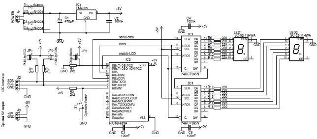
This circuit is easy to understand. First there is a power supply. It accepts an AC or a DC input voltage. This voltage is then rectified by the 4 diodes. Then the 7805 regulator converts the voltage to a stable 5 VDC voltage. The component has some surrounding capacities to remove the high-frequency noise.
The circuit is controlled by a PIC microcontroller: the 16F628A. This PIC uses a 4 MHz internal oscillator, this avoids the need for any external oscillating components. The PIC uses the following connections:
The I2C scanner uses two 7-segment displays to show the result. Each segment is driven separately so I would have needed 14 I/O pins on my microcontroller. I implemented two shift registers to avoid this. The microcontroller will transmit some serial data to them. To do this the PIC will generate 14 clock pulses. A data bit (1/0) is transferred to the shift registers during each clock pulse. The shift registers are placed in cascade: the second register gets its data from the first register.
The I2C lines are pulled-up to the 5 VDC line, this is required by the I2C specifications. You should connect this circuit only to 5 VDC operated I2C systems. It is possible to connect them to 3.3 V systems by using a voltage adjustment circuit. The image below shows the circuitry that is required to do so (See my FEZ To K8000 Project).

The circuit is very easy to use as it only has one push button. I didn't make any software option to turn the device off. You can do this by simply disconnecting the power supply (You could add a switch for this).
Here is a complete description of the procedure the device will follow to scan the I2C bus:
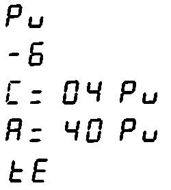
The following image gives an idea on the possible output sequences you can encounter. This scan has resulted in 4 addresses, one of them is 0x40 (the other 3 results are not shown here). At the end the "te" appears to indicate the end of the scan.
My I2C bus scanner has some additional features: you can remove jumpers JP1 and JP2 to disable the pull-up resistors. They are not required when you connect the scanner to a circuit that already has pull-up resistors. The I2C bus needs these pull-up resistors for both SCL and SDA lines to make sure they are "high" when the bus is not in use.
The jumper JP3 affects how the found addresses are displayed: when the JP3 is installed all found addresses are shifted one bit to the left. So the real hexadecimal address 0x38 (0b00111000) will be shifted to (0b01110000). I will explain the reason with an example. The picture below is a snippet from the datasheet of the IC PCF8574AP (I2C Port Expander).
I2C uses 7-bit addresses. The 8th bit of the addressing byte is a R/W (read/write) bit to indicate the kind of operation you want to perform. The data sheets often show this 8th bit as a zero, so I added an option to show these addresses as they would appear in the datasheet.
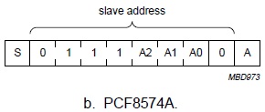
Let's assume the A0,A1 and A2 are set to 0. Then the hardware address that is shown is 0b01110000 (0x70). The bit at the right "0" (LSB: Least Significant Bit) doesn't actually belong to the hardware address, but it is a read/write byte to specify the type of I2C operation. So the real hardware address is 0b0111000 (0x38). The jumper JP3 will allow you to select how the address will be shown.
I wrote the PIC's firmware with the Lite-version of High-Tech C. I won't explain the program in detail, but the source code is well commented.
The PIC 16F628A doesn't support hardware I2C so I had to write my own I2C functions in software. These functions will emulate open-collector outputs on the PIC: the software will change them from inputs to outputs when required.
You can download the High-Tech C source files together with the data sheets of the used components.
Copyright ©1998-2022 Vanderhaegen Bart - last modified: August 24, 2013
