FEZ ULTIKIT - [FEZ Accu Test]
In the image below you can find the schematic diagram for the circuit. You can also download it as PDF.
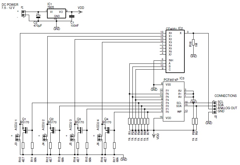
The circuit consists of a few basic parts: the power supply, the discharger(s), an analog multiplexer and a controller.
The power supply delivers a stable +5VDC voltage. Some capacitors were added to decrease the noise. This 5VDC is used to power the rest of the system.
There are four connectors to connect the AA-batteries to: The "+" connection of each battery is brought to an input of the analog multiplexer (the IC CD4051). The "-" is just connected with the GND of the device.
I used an N-channel FET to control the discharging of the batteries: when the FETs are conducting the current from the battery flows through the Drain-Source junction of each FET trough the resistor of 4.7 Ω. This will create a current of about 150 to 200 mA.
As you probably know FETs are voltage controlled: they are only conducting when there is a voltage between the Gate and the Source connection. This voltage is controlled by the PCF8574 IC, an I2C port expander. Basically you can control the outputs of the PCF8574 by sending I2C commands to it.
The PCF8574 not only controls the FETs but it also controls the address selection of the multiplexer IC: it chooses which battery voltage is passed to the output. There are 3 address lines (A0,A1,A2).
A FET can be compared with a switch: when this "switch" is opened almost no current is drawn from the batteries. Because of this the input of the analog multiplexer contains the unloaded battery voltage.
When you now apply a voltage to the gate of the FET its Drain-Source channel is opened: now a current can flow from the battery to the GND. In this case the loaded battery voltage is present at the respective input of the analog multiplexer.
The question is: how much current will be drained from the batteries? This current can be calculated using Ohm's law: I = U / R. U is the battery voltage which has an expected value of 1 to 1.5 Volt. R is the resistance: the resistance of 4.7 Ω. But this is not the total resistance as the drain-source channel of the FET also has a certain resistance: For the BS170 this resistance is about 1.2 to 5 Ω (this number comes from the datasheet). This resistance is placed in series with the resistance of 4.7 Ω, what results in a total resistance of 5.9 to 9.7 Ω. If you do the math you will come to a current range of 100 to 250 mA.
One last item I want to discuss is the voltage which will be present at the gate of the FETs. First of all you have to know the controller IC PCF8574 has open-drain outputs: they don't give any voltage. You have to connect a pull-up resistor to them: I have used 7 of them, each with a resistance of 1 kΩ. The PCF8574 will (or won't) connect these with the ground. This means the gates of each BS170 FET will have either 0V or approximately 5V on them. (actually it will be more like 4.92 V as the pull-up resistors and the 68k resistors are forming a voltage divider. More than 98% of the voltage will be over the 68k resistors). The expected gate-voltage of each FET should be 0.7 V at most, which causes the FETs to be in fully conduction: For the BS170 the Ugs voltage must be higher than 3V for full conduction.
Theoretically you can increase the discharging current by lowering the values of the 4 resistors (R10,R12,R14,R16).The BS170 can handle currents of up to 500 mA. A current at which the dissipation in the FETs would still be within acceptable limits.
Four FETs will regulate the discharging of the batteries. You can control them by sending I2C commands to the PCF8574. The output value from the batteries is brought to a multiplexed output whose value can be selected by setting the desired address on the address inputs. This is also done by sending a command to the PCF8574.
![]()
![]()
Copyright ©1998-2022 Vanderhaegen Bart - last modified: August 24, 2013
